- 您现在的位置:买卖IC网 > Sheet目录3882 > PIC18F4539-I/ML (Microchip Technology)IC MCU FLASH 12KX16 EE A/D 44QFN
2002 Microchip Technology Inc.
Preliminary
DS30485A-page 21
PIC18FXX39
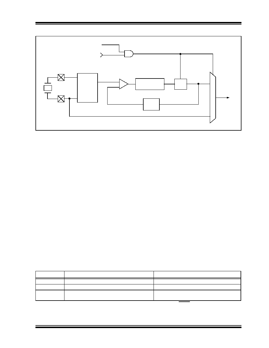
FIGURE 2-5:
PLL BLOCK DIAGRAM
2.5
Effects of SLEEP Mode on the
On-Chip Oscillator
When the device executes a SLEEP instruction, the
oscillator is turned off and the device is held at the
beginning of an instruction cycle (Q1 state). With the
oscillator off, the OSC1 and OSC2 signals will stop
oscillating. Since all the transistor switching currents
have been removed, SLEEP mode achieves the lowest
current consumption of the device (only leakage cur-
rents). Enabling any on-chip feature that will operate
during SLEEP will increase the current consumed dur-
ing SLEEP. The user can wake from SLEEP through
external RESET, Watchdog Timer Reset, or through an
interrupt.
2.6
Power-up Delays
Power-up delays are controlled by two timers, so that
no external RESET circuitry is required for most appli-
cations. The delays ensure that the device is kept in
RESET, until the device power supply and clock are
stable. For additional information on RESET operation,
see Section 3.0.
The first timer is the Power-up Timer (PWRT), which
optionally provides a fixed delay of 72 ms (nominal) on
power-up only (POR and BOR). The second timer is
the Oscillator Start-up Timer (OST), intended to keep
the chip in RESET until the crystal oscillator is stable.
With the PLL enabled (HS/PLL Oscillator mode), the
time-out sequence following a Power-on Reset is differ-
ent from other Oscillator modes. The time-out
sequence is as follows:
1.
The PWRT time-out is invoked after a POR time
delay has expired.
2.
The Oscillator Start-up Timer (OST) is invoked.
However, this is still not a sufficient amount of
time to allow the PLL to lock at high frequencies.
3.
The PWRT timer is used to provide an additional
fixed 2 ms (nominal) time-out to allow the PLL
ample time to lock to the incoming clock
frequency.
TABLE 2-2:
OSC1 AND OSC2 PIN STATES IN SLEEP MODE
MUX
VCO
Loop
Filter
÷4
Crystal
Osc
OSC2
OSC1
PLL Enable
FIN
FOUT
SYSCLK
Phase
Comparator
(from Configuration
HS Osc
bit Register)
OSC Mode
OSC1 Pin
OSC2 Pin
ECIO
Floating
Configured as PORTA, bit 6
EC
Floating
At logic low
HS
Feedback inverter disabled, at quiescent
voltage level
Feedback inverter disabled, at quiescent
voltage level
Note:
发布紧急采购,3分钟左右您将得到回复。
相关PDF资料
PIC18F4439-I/ML
IC MCU FLASH 6KX16 EE A/D 44QFN
PIC18F2439-I/SO
IC MCU FLASH 6KX16 EE A/D 28SOIC
PIC16F687-I/SO
IC PIC MCU FLASH 2KX14 20SOIC
PIC16F877AT-I/PTG
IC MCU FLASH 8KX14 W/AD 44 TQFP
PIC16F877A-I/LG
IC MCU FLASH 8KX14 W/AD 44PLCC
PIC12LC509AT-04I/MF
IC MCU OTP 1KX12 LV 8-DFN
PIC12C509AT-04I/MF
IC MCU OTP 1KX12 8-DFN
PIC24F08KL301-I/SS
IC MCU 16BIT 8KB FLASH 20-SSOP
相关代理商/技术参数
PIC18F4539-I/P
功能描述:8位微控制器 -MCU 24KB 1408 RAM 32 I/O RoHS:否 制造商:Silicon Labs 核心:8051 处理器系列:C8051F39x 数据总线宽度:8 bit 最大时钟频率:50 MHz 程序存储器大小:16 KB 数据 RAM 大小:1 KB 片上 ADC:Yes 工作电源电压:1.8 V to 3.6 V 工作温度范围:- 40 C to + 105 C 封装 / 箱体:QFN-20 安装风格:SMD/SMT
PIC18F4539-I/P
制造商:Microchip Technology Inc 功能描述:IC 8BIT FLASH MCU 18F4539 DIP40
PIC18F4539-I/PT
功能描述:8位微控制器 -MCU 24KB 1408 RAM 32 I/O RoHS:否 制造商:Silicon Labs 核心:8051 处理器系列:C8051F39x 数据总线宽度:8 bit 最大时钟频率:50 MHz 程序存储器大小:16 KB 数据 RAM 大小:1 KB 片上 ADC:Yes 工作电源电压:1.8 V to 3.6 V 工作温度范围:- 40 C to + 105 C 封装 / 箱体:QFN-20 安装风格:SMD/SMT
PIC18F4539IPT
制造商:MICRO CHIP 功能描述:NEW
PIC18F4539T-E/ML
功能描述:8位微控制器 -MCU 24KB 1408 RAM 32 I/O RoHS:否 制造商:Silicon Labs 核心:8051 处理器系列:C8051F39x 数据总线宽度:8 bit 最大时钟频率:50 MHz 程序存储器大小:16 KB 数据 RAM 大小:1 KB 片上 ADC:Yes 工作电源电压:1.8 V to 3.6 V 工作温度范围:- 40 C to + 105 C 封装 / 箱体:QFN-20 安装风格:SMD/SMT
PIC18F4539T-E/PT
功能描述:8位微控制器 -MCU 24KB 1408 RAM 32 I/O RoHS:否 制造商:Silicon Labs 核心:8051 处理器系列:C8051F39x 数据总线宽度:8 bit 最大时钟频率:50 MHz 程序存储器大小:16 KB 数据 RAM 大小:1 KB 片上 ADC:Yes 工作电源电压:1.8 V to 3.6 V 工作温度范围:- 40 C to + 105 C 封装 / 箱体:QFN-20 安装风格:SMD/SMT
PIC18F4539T-I/ML
功能描述:8位微控制器 -MCU 24KB 1408 RAM 32 I/O RoHS:否 制造商:Silicon Labs 核心:8051 处理器系列:C8051F39x 数据总线宽度:8 bit 最大时钟频率:50 MHz 程序存储器大小:16 KB 数据 RAM 大小:1 KB 片上 ADC:Yes 工作电源电压:1.8 V to 3.6 V 工作温度范围:- 40 C to + 105 C 封装 / 箱体:QFN-20 安装风格:SMD/SMT
PIC18F4539T-I/PT
功能描述:8位微控制器 -MCU 24KB 1408 RAM 32 I/O RoHS:否 制造商:Silicon Labs 核心:8051 处理器系列:C8051F39x 数据总线宽度:8 bit 最大时钟频率:50 MHz 程序存储器大小:16 KB 数据 RAM 大小:1 KB 片上 ADC:Yes 工作电源电压:1.8 V to 3.6 V 工作温度范围:- 40 C to + 105 C 封装 / 箱体:QFN-20 安装风格:SMD/SMT